To draw V-I characteristics of a semiconductor diode (Ge, Si) and determine its knee voltage
Theory
Forward bias
The positive terminal of a battery is connected to p-side of a diode and the negative terminal of the battery is connected to the negative terminal of the battery. The majority electrons from the n-side and the majority holes from p-side are pushed towards the junction and reduces the depletion layer. The depletion layer becomes thin and at a certain value of forward biasing voltage, the depletion layer vanishes. The charge carriers cross the junction and make the current flow.
Procedure
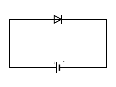
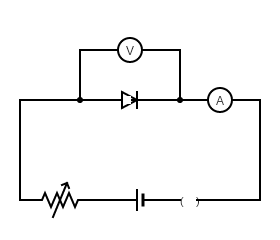
i. All circuit connections are made according to the figure.
ii. In forward bias characteristics, the p-region is connected with positive terminal and n-region is connected to negative terminal of the battery.
iii. 10 to 15 readings are taken to study the forward bias characteristics of the diode.
Results
| No. of observations | Voltage in V | Current in mA |
| 1 | ||
| 2 | ||
| 3 | ||
| 4 | ||
| 5 | ||
| 6 | ||
| 7 | ||
| 8 | ||
| 9 | ||
| 10 |
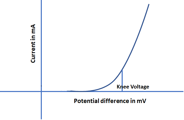
Knee voltage from graph = _________ V
Precautions
i. The current in the diode should not be greater than the maximum rated current.
ii. In forward bias condition, the p side of the diode should be connected to positive terminal and the n side of the diode should be connected to negative terminal of the battery.
iii. All connections should be tight.
iv. At the turning point, more reading should be taken to draw the graph properly.
Viva questions on V-I characteristics of p-n junction diode experiment | Practical
1. What is a Semiconductor?
Answer: It is a substance with conductivity in between metals and insulators.
2. What is intrinsic semiconductor?
Ans: Intrinsic or pure semiconductor are free from any impurities.
3. What is extrinsic semiconductor?
Ans: When impurities are added with pure semiconductor, it becomes impure or extrinsic semiconductor.
4. What are the different types of extrinsic semiconductor?
Ans: Depending upon the nature of impurities, extrinsic semiconductors are divided in two types – n-type and p-type.
5. How to make n-type and p-type semiconductor?
Ans: Pentavalent impurity (Arsenic, Antimony, Phosphorus) is added with intrinsic semiconductor to make n type semiconductor and trivalent impurity (Boron, indium) is added to make p-type semiconductor.
6. What are majority and minority charge carriers in n-type and p-type semiconductor?
Ans: In n-type semiconductor,
majority carrier: electrons
minority carrier: Holes
In p-type semiconductor,
majority carrier: Holes
minority carrier: electrons
7. What is the effect of temperature on conductivity of a semiconductor?
Ans: The conductivity increases ( resistivity decreases) with increase in temperature of a semiconductor.
8. What is a p-n junction diode?
Ans: When one side of a semiconductor is doped with pentavalent impurity and other side is doped with trivalent impurity atoms, a p-n junction is formed.
9. What is forward and reverse biasing of a semiconductor diode?
Ans: When the p-side of a diode is connected with positive terminal and n-side is connected with negative terminal of external source, it is called forward biasing.
When the n-side of a diode is connected with positive terminal and p-side is connected with negative terminal of external source, it is called reverse biasing.
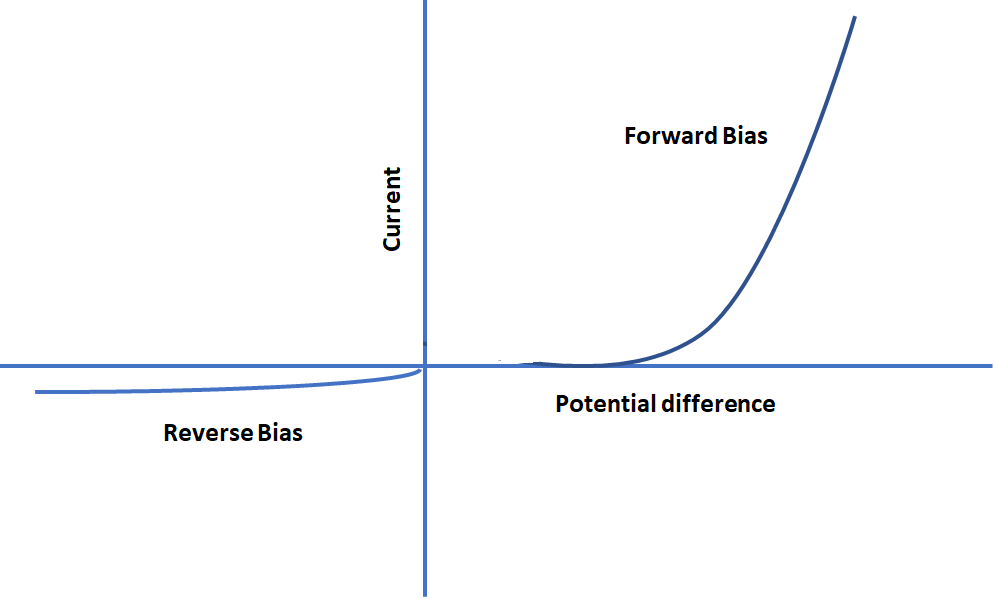
10. Draw the V-I characteristics of a p-n junction diode in forward bias and reverse bias condition.
Ans:
| More laboratory experiments on Physics | click here |
| Find topic wise physics questions | click here |